10+ Pcb Footprint Simple Dan Minimalis
Poin pembahasan 10+ Pcb Footprint Simple Dan Minimalis adalah :
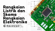
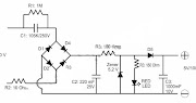
10+ Pcb Footprint Simple Dan Minimalis. Berikut Penjelasan lengkap tentang fungsi komponen-komponen skema pcb dari yang aktif hingga pasif, prinsip cara kerjanya serta simbol yang wajib difahami. Perhatikan komponen skema pcb jenis resistor berikut yang dilengkapi dengan gambar. Simak ulasan terkait skema pcb dengan artikel 10+ Pcb Footprint Simple Dan Minimalis berikut ini

pcb footprints distinguido comze com Sumber : distinguido.comze.com

PCB footprint generator Sumber : dlharmon.com

How to Create Perfect SMT Footprints in PCB Layout Sumber : www.allpcb.com

pcb footprints distinguido comze com Sumber : distinguido.comze.com

Propeller 2 Package Information PCB Footprint Sumber : forums.parallax.com

PCB Footprint Creation 2 3 of Part Creation Tutorial Sumber : www.youtube.com

Homepage of Dr Stefan Salewski Sumber : www.ssalewski.de

PCB Final FootPrint Resources EasyEDA Sumber : easyeda.com

Download preactivated version downloadvector Sumber : downloadmango.weebly.com

PCB Artist Northwestern Mechatronics Wiki Sumber : hades.mech.northwestern.edu

What s Good about OrCAD Apps Symbol and Footprint Sumber : community.cadence.com

Support for Parameters in PCB Footprints Online Sumber : www.altium.com

EasyEDA Tutorial Sumber : docs.easyeda.com

PCB Design Tool automates generation of PCB footprint Sumber : news.thomasnet.com

Missing Information of CC2564x Footprint PCB Land Pattern Sumber : e2e.ti.com
samacsys, component search engine, download library eagle full, kumpulan library eagle, snapeda, www instapart net, library altium 18, library altium 16,
10+ Pcb Footprint Simple Dan Minimalis. Berikut Penjelasan lengkap tentang fungsi komponen-komponen skema pcb dari yang aktif hingga pasif, prinsip cara kerjanya serta simbol yang wajib difahami. Perhatikan komponen skema pcb jenis resistor berikut yang dilengkapi dengan gambar. Simak ulasan terkait skema pcb dengan artikel 10+ Pcb Footprint Simple Dan Minimalis berikut ini
pcb footprints distinguido comze com Sumber : distinguido.comze.com
PCBL PCB Library Expert
PCB footprint generator Sumber : dlharmon.com
PCB Footprints Designing and Building PCB Footprints
08 10 2020 A footprint also called a land pattern is used during board layout and is where an electronic component gets soldered onto the PCB It consists of several layers of information including the copper lands silkscreen the text and shapes you
How to Create Perfect SMT Footprints in PCB Layout Sumber : www.allpcb.com
PCB Footprints OpenCircuits
The PCB Library Expert Enterprise is a powerful CAD library development tool powered by our own proprietary CAD LEAP TM Technology Libraries Enhanced with Automated Preferences It is packed with very powerful advanced library management features that cuts footprint creation costs by
pcb footprints distinguido comze com Sumber : distinguido.comze.com
Creating the PCB Footprint Altium Designer 20 0 User
Propeller 2 Package Information PCB Footprint Sumber : forums.parallax.com
What does a footprint mean in PCB design Quora
Once selected the schematic symbols PCB footprints and 3D models are immediately available for use and placement If a part doesn t have a symbol or footprint when clicking on the icon to download you can build one or request a part To build simply use the wizard from SamacSys to create both the schematic symbol and PCB footprint
PCB Footprint Creation 2 3 of Part Creation Tutorial Sumber : www.youtube.com
Footprint electronics Wikipedia
PCB Footprint Resources In order to accurately design your footprints you really need access to the IPC 7351 standard However IPC has teamed with PCB Matrix and is distributing a free Land Pattern Viewer This tool is essential for design land patterns and will save you hundreds of hours This tool will provide the dimensions for pad
Homepage of Dr Stefan Salewski Sumber : www.ssalewski.de
SnapEDA Free PCB Footprints and Schematic Symbols
A footprint or land pattern is the arrangement of pads in surface mount technology or through holes in through hole technology used to physically attach and electrically connect a component to a printed circuit board The land pattern on a circuit board matches the arrangement of leads on a component
PCB Final FootPrint Resources EasyEDA Sumber : easyeda.com
Easy Way to Get Symbols PCB Footprints 3D Models Mouser
11 12 2020 Updating a PCB Footprint Updating a PCB Footprint can be done in two ways Pushing the PCB from the PCB Library or by Pulling from the PCB Editor Pushing a PCB Footprint update takes a selected footprint s from the PCB Library and uses it to update all open PCB documents containing that footprint
Download preactivated version downloadvector Sumber : downloadmango.weebly.com
PCB Artist Northwestern Mechatronics Wiki Sumber : hades.mech.northwestern.edu
What s Good about OrCAD Apps Symbol and Footprint Sumber : community.cadence.com
Support for Parameters in PCB Footprints Online Sumber : www.altium.com
EasyEDA Tutorial Sumber : docs.easyeda.com
PCB Design Tool automates generation of PCB footprint Sumber : news.thomasnet.com
Missing Information of CC2564x Footprint PCB Land Pattern Sumber : e2e.ti.com


0 Comments